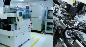
BIWIN IC Packaging Process
Wafer Thinning
Function:Wafer thinning is the process of grinding the back side of a wafer to reduce it to a suitable thickness required for packaging.
Equipment model:TSK PG3000RM
Capacity:
- 8-inch, 12-inch wafer processing capacity
- Maximum thinning 25 um
- The wafer thickness error ±5 um
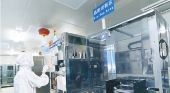
Wafer Cutting
Function:Wafer cutting is the process of cutting and separating the dies on a wafer.
Equipment model:TSK AWD-300TXB & Disco DFD6361
Capacity:
- 12-inch wafer processing capability
- The minimum cutting channel can reach 45 um
Wafer Mounting
Function:Place each die in the lead frame or substrate, and stick and fix it in Epoxy
Equipment model:Hitachi DB-830 Plus
Capacity:
- Mounting accuracy ±15 u
- Minimum die size: 0.5 × 0.5 mm
- Capable to produce dispensing and DAF
Bonding Wire
Function:The die bonding pad is welded to the substrate bonding pad or the I/O lead in the lead frame using high purity gold, copper or alloy wire.
Equipment model:K &S Iconn
Capacity:
- Gold wire with diameter of 0.6 mil can be produced
- Copper wire and alloy wire can be produced massively
Plastic Package
Function:Seal the dies at the front end that completes the welding wire, to protect the die and welding wire from damage, pollution and oxidation.
Equipment model:Towa Auto Mold Y-1
Capacity:
- Automatic production machine with vacuum system
- Mass production machine plate size is 240 × 74 mm
Tin-ball Welding
Function:Weld the fixed-specification tin ball on the machine plate which has completed molding.
Equipment model:AurIgIn Au 800 A Soldier Ball Mounter-Cell 2
Capacity:
- The minimum diameter of mounted tin ball is 0.25 mm
- Minimum spacing of tin balls is 0.4 mm
Cutting Molding
Function:Separate the packaged chip from the substrate or lead frame and form a pre-designed shape.
Equipment model:HAMI semiconductor – 3000; ASM Trim Form MP209
Capacity:
- The contour accuracy of the product can be controlled within ±50 um
- Capable to achieve cutting of product with“ opposite” shape