

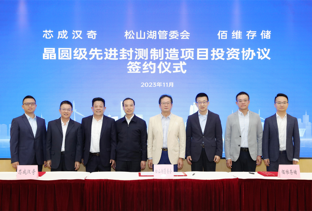
Recently, the wafer-level advanced packaging and testing manufacturing project of BIWIN Storage Technology Co., Ltd. officially landed in the Dongguan Songshan Lake High-tech Industrial Development Zone, and the signing ceremony was successfully held in Dongguan City. BIWIN's Chairman, Sun Chengsi, General Manager, He Han, Founder, Sun Rixin, and Liu Kunqi, General Manager of Huizhou BIWIN, a subsidiary of BIWIN Storage Technology Co., Ltd., and Guangdong Xincheng Hanqi (the main implementation entity of this project) attended the signing ceremony. The solemn moment of contract signing was witnessed by Lü Chengqi, Deputy Secretary of the Dongguan Municipal Party Committee and Mayor of Dongguan City, Liu Wei, Deputy Secretary of the Dongguan Municipal Party Committee and Secretary of the Songshan Lake Party Working Committee, Ouyang Nanjiang, Deputy Secretary of the Songshan Lake Party Working Committee and Director of the Management Committee, as well as Chen Shunjiao, Director of the Dongguan Investment Promotion Bureau.
In addition, heavyweight guests from academia, finance, and the industry chain also attended this signing ceremony. Professor Chen Xin, the former Party Secretary and President of Guangdong University of Technology, and the current Director of the National Key Laboratory of the Guangdong University of Technology, Liang Guozhi and Wang Zanzhang, Partners of Fortune Venture Capital, Sun Chen, Director of the Shenzhen Branch of China Development Bank, Li Hao, Deputy Director, Wu Jinrong, Director of the Shenzhen Branch of the Export-Import Bank of China, and Li Yang, Chairman and General Manager of Guangzhou Smarter Micro, were among the distinguished guests who attended the signing ceremony.
Wafer-level advanced packaging and testing is an intermediate semiconductor manufacturing process between front-end wafer manufacturing and back-end packaging and testing. It employs processes such as lithography, etching, electroplating, PVD, CVD, CMP, Strip, and other front-end wafer manufacturing processes to achieve process technologies such as Bumping, Re-distribution Layer (RDL), Fan-in, Fan-out, and Through Silicon Via (TSV). This not only allows chips to be directly packaged on wafers, saving physical space but also enables the integration of multiple chips on the same wafer, achieving higher integration. Landing the wafer-level advanced packaging and testing project is conducive to BIWIN’s products achieving greater bandwidth, higher speed, more flexible heterogeneous integration, and lower energy consumption, empowering customers in applications such as mobile consumer electronics, high-end supercomputing, gaming, artificial intelligence, and the Internet of Things.
Overall, BIWIN has the technical support and competitive advantages required to implement this project. Thanks to its deep accumulation in the field of advanced packaging and testing, BIWIN has mastered advanced packaging processes such as 16-layer stacked Die, 30-40μm ultra-thin Die, and multi-chip heterogeneous integration, providing support for the innovation and large-scale production of NAND, DRAM, and SiP packaging products. Currently, BIWIN has established a well-structured, internationally oriented professional wafer-level advanced packaging technology and operation team and has reached strategic cooperation with Guangdong University of Technology to jointly promote the development of wafer-level advanced packaging technology in the Greater Bay Area, empowering project implementation and business success.
Wafer-level advanced packaging and testing is one of the key development directions in the current semiconductor industry. Its widespread application will further drive the development and intelligence of electronic devices, helping the integrated circuit industry achieve benign development with high computing power and low power consumption. Landing the wafer-level advanced packaging and testing project is a forward-looking layout of BIWIN in response to the development needs of advanced memory, as well as the trend of storage and logic integration technology. The project aims to set a benchmark for advanced testing in the Greater Bay Area. The company actively promotes WIN-WIN cooperation with IC design manufacturers, wafer manufacturers, end customers, and other industry partners to contribute to the construction and enhancement of the integrated circuit industry scale and technological level in the Greater Bay Area.