

SiP China 2023 | BIWIN: Moving towards Wafer-level Packaging and Testing Based on Advanced Packaging and Testing
Recently, Liu Kunqi, general manager of Huizhou BIWIN, was invited to give a speech on the theme of "Analysis of Storage Packaging in SiP" at the SiP China 2023, sharing BIWIN's technical layout and typical application cases in the field of advanced packaging & testing and discussing its development trend with industry leaders.
Integration of R&D, packaging and testing
Advanced packaging and testing is the key link
Mr. Liu first introduced the business layout and advanced packaging and testing capabilities of BIWIN. “BIWIN has built a business model integrating R&D, packaging and testing around the semiconductor industry chain. The advanced packaging and testing business is the key link to endow BIWIN with competitive advantages of strong product reliability, high quality, and stable delivery. It’s the solid foundation for BIWIN's long-term development.” Mr. Liu said.
With the support of advanced packaging and testing technology, BIWIN has innovatively developed a series of memory chips in special sizes, which feature "small, precision, low power consumption, high performance and high stability", such as the ultra-small size eMMC and ePOP launched by BIWIN. These products are ideal storage solutions for wearable devices. They stand out from the fierce competition, successfully entered the supply chain system of global technology giants, and received positive responses from customers and the market.
Advanced packaging and full-stack chip test development capabilities
Producing products with high reliability and excellent quality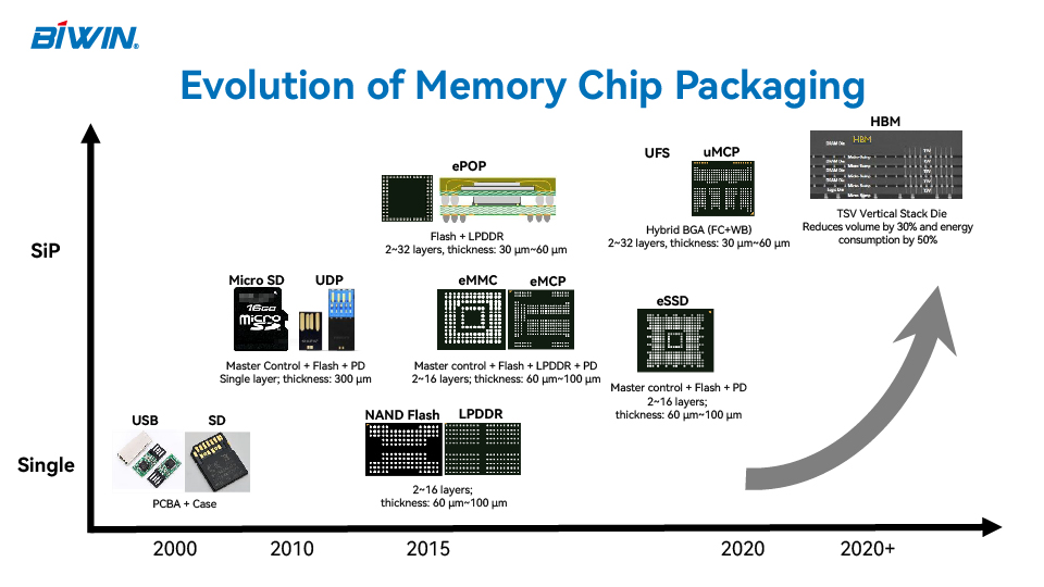
Mr. Liu's mentioned that in the multiple rounds of technological innovation, the packaging technology has been continuously developing in the direction of large capacity, thin volume, and high quantity, and has gradually become a key means to improve chip performance and stability. In the field of packaging, BIWIN has maturely mastered laser stealth dicing, ultra-thin Die bonding, lead wires bonding of ultra-low wire arcs, compression molding process, FC process, CSP process, POP, PIP and 3D SiP, and packaging electromagnetic shielding and other process technologies, and has the mass production capacity of advanced processes such as 16-layer Die, 30 μm~40 μm ultra-thin Die, and multi-chip heterogeneous integration, which makes the memory chip have strong market competitiveness in terms of volume, heat dissipation, electromagnetic compatibility, reliability, and storage capacity.
He emphasized that chip testing is an important link to ensure the product quality of memory chips. BIWIN has full-stack chip test development capabilities from test equipment hardware development, test algorithm development, and test automation software platform development, covering Flash chip test, memory chip function test, burn-in test, DRAM automation test, DRAM system test, and more. At the same time, through years of product development, testing, and application updates, BIWIN has accumulated a rich and diverse product and chip test algorithm library on the above-mentioned independent platform, and conducts rigorous testing of product reliability to ensure excellent performance and stable quality for products.
Comply with the development of advanced memory
Build wafer-level advanced packaging and testing
With the rapid development of mobile consumer electronics, high-end supercomputing, artificial intelligence and Internet of Things technologies, the market requires advanced memory products with greater bandwidth, higher speed, and lower power consumption. Semiconductor wafer-level advanced packaging and testing, as an intermediate process between front-end wafer manufacturing and back-end packaging and testing, is one of the key development directions in the field of semiconductor technology. Both advanced DRAM chips and NAND controller chips need to use wafer-level packaging and testing technology.
In order to meet the development needs of advanced memory, BIWIN is stepping up the construction of wafer-level packaging and testing capabilities, and has built a complete and international advanced packaging and testing technology team. At present, the semiconductor industry in the Greater Bay Area has obvious advantages in front-end processes such as IC design and wafer manufacturing. BIWIN's establishment of wafer-level advanced packaging and testing capabilities will promote the supplementary chain and strong chain of the semiconductor industry in the Greater Bay Area, and build a complete semiconductor industry ecology.
Summary
BIWIN specializes in the field of semiconductor memory, has profound technical strength and rich industry experience, covers a wide range of application fields with a complete product matrix, and its memory chip packaging and testing technology has reached the domestic leading level. In the future, BIWIN will continue to increase investment in technical fields such as storage medium characteristics research, chip design, firmware / software / hardware development, advanced packaging and testing, storage test equipment and algorithm development, extend BIWIN's value chain, and enhance BIWIN's core competitiveness to provide customers with more efficient and high-quality storage solutions.