

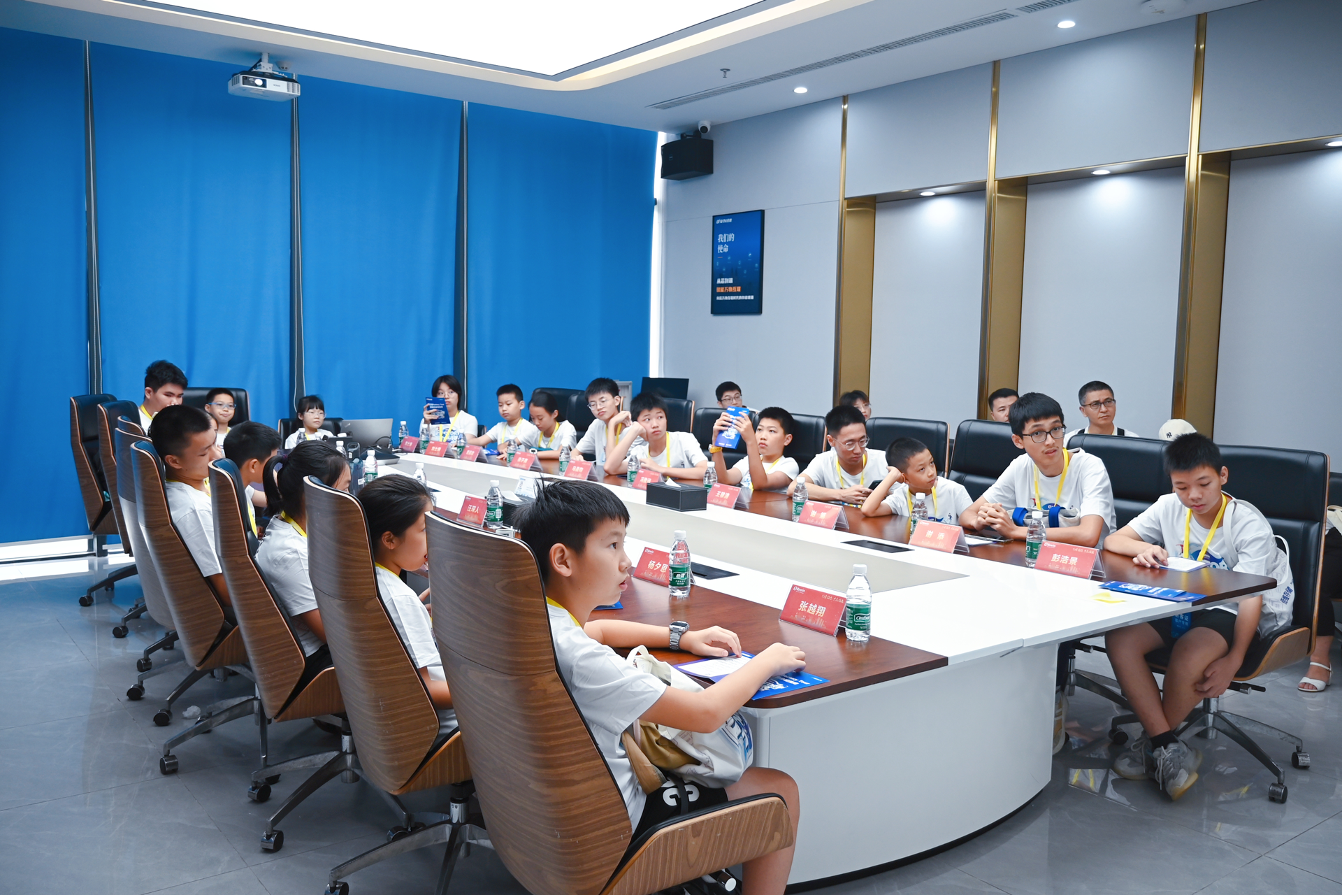
As summer vacation rolls around again, BIWIN's "Factory Tour" Open Day made a brilliant return, shining a technological beacon to captivate visionary and creative young individuals. The Third "Factory Tour" Open Day, held on July 29-30 and August 25, wrapped up successfully at BIWIN's advanced packaging and testing manufacturing base in Huizhou. The event, which took place over five sessions, welcomed more than 170 parents and youths who got a close-up look at the world of semiconductor memory packaging and testing, unveiling the mysteries behind "chip" manufacturing.

Event Highlights
Getting to Know Chips
How many stages must sand undergo to become high-tech chips? How do chips lead us into the AI era? What does a chip look like magnified 3,000 times? How are high-quality chips forged? To provide visitors with a comprehensive view of storage chips, BIWIN's trainers took on the role of tech guides, presenting a complete overview of the chip's journey from raw materials to finished product, as well as the whole picture of the division of the industry chain and technological evolution.
Exploring the Workshop
Brimming with excitement about their first acquaintance with chips, parents and young guests started their visit in the packaging workshop, where they gain an in-depth knowledge of the advanced packaging processes, including wafer grinding, wafer mounting, wire bonding, substrate molding, laser marking, final cutting, and aging test. The intricacy and sophistication of chip manufacturing have sparked deep interest among the young visitors, and many of them expressed a desire to become chip manufacturing engineers in the future.

Hands-On Experiments
The exploring group then moved on to the testing areas, including the environmental reliability, physical reliability, compatibility, and environmental testing labs, as well as the SSD testing area. The young discoverers stepped into the shoes of "one-day engineers", and got immersed in hands-on operations with microscopes, tensile and pressure tests. Through explanations and demonstrations by professionals, they acquired an in-depth knowledge of how chips are rigorously tested to deliver superior performance and reliability.

Technology is reshaping the world, and innovation is steering the future. Semiconductor storage and packaging technologies are pivotal in driving the advancement of AI and other sophisticated applications. The integrated circuit industry, the hub of technological innovation, has become a highly sought-after field for countless aspiring youngsters. As a prominent storage and packaging company in China, BIWIN remains steadfast in fulfilling its social responsibilities. For the past three consecutive years, BIWIN has sown the seeds of interest in the semiconductor industry among the youth through its Semiconductor IC Packaging and Testing Factory Tour for Youth, which has sparked their curiosity for cutting-edge technologies and strengthened their resolve to pursue their "chip" dreams. BIWIN looks forward to collaborating with more outstanding youth in exploring the limitless possibilities of China's "chip" era!