

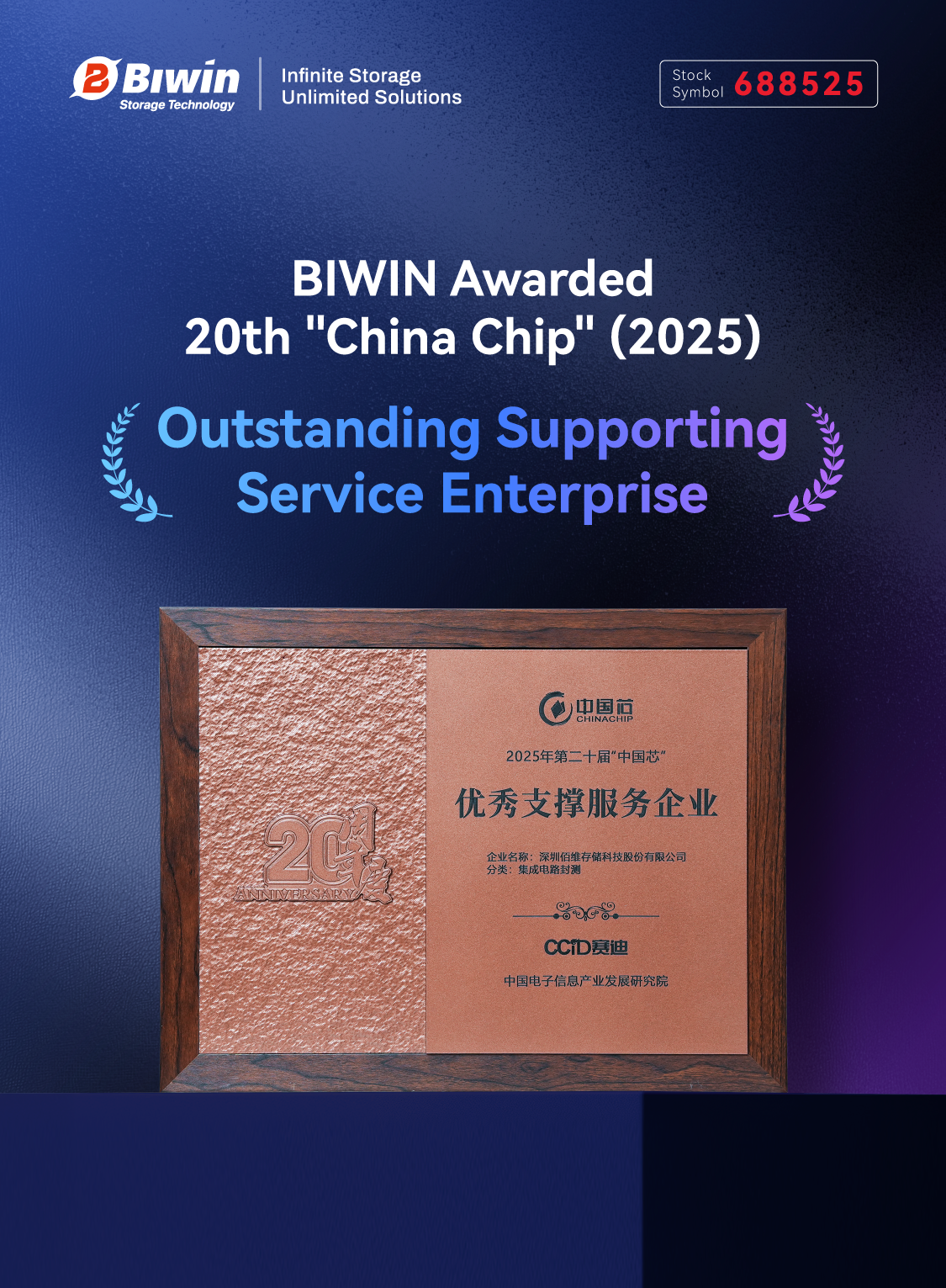
The 20th “China Chip” Outstanding Product Awards Ceremony – guided by the Ministry of Industry and Information Technology and hosted by the China Center for Information Industry Development (CCID) – was recently held, with the final results officially announced. For the second consecutive year, BIWIN has been honored with the title of “20th ‘China Chip’ Outstanding Supporting Service Enterprise.”
As one of the most influential and authoritative awards in China’s integrated circuit (IC) industry, the “China Chip” Outstanding Product Awards recognize leading achievements across the sector. Receiving this honor two years in a row underscores BIWIN’s sustained innovation in advanced packaging and testing technologies, as well as its significant contributions to supporting the coordinated, high-quality development of the entire industry ecosystem.
Advanced Packaging Leads New Innovations: Mini SSD and ePOP Reshape Edge AI Storage
At this year’s awards, BIWIN was recognized as a “‘China Chip’ Outstanding Supporting Service Enterprise” for its groundbreaking Mini SSD and ePOP storage solutions. These two products exemplify BIWIN’s strategy of leveraging advanced packaging technology to deliver highly differentiated, ultra-compact, high-performance storage that opens up new application possibilities.
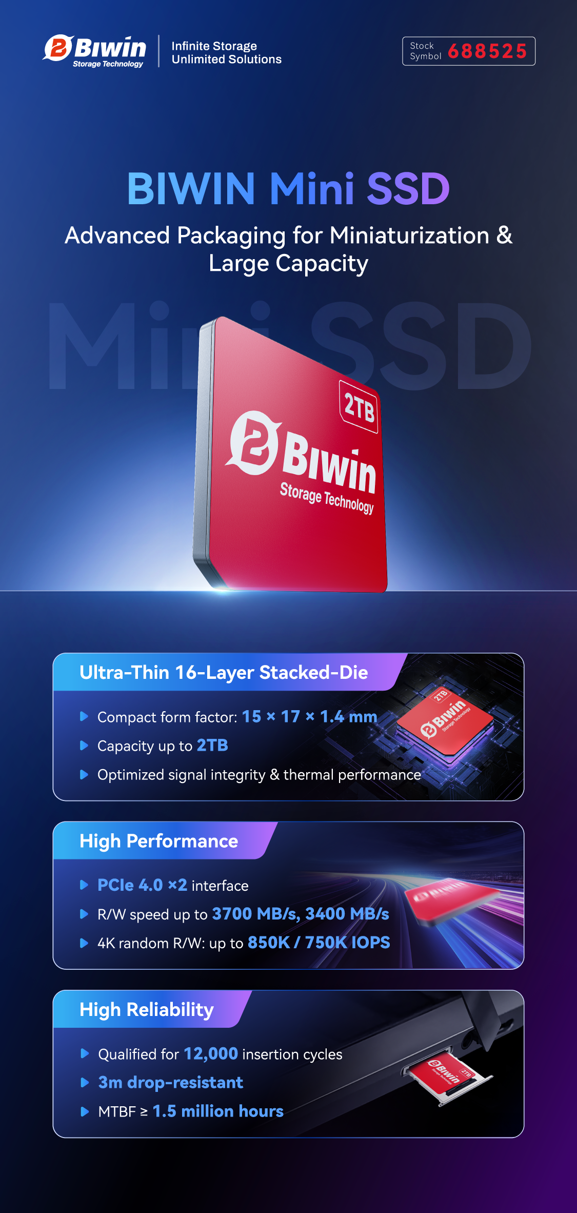
By using a high-integrated system-in-package (SiP), Mini SSD packs critical components including controller, NAND, and power management ICs into a footprint smaller than half a coin. Through 16-layer ultra-thin die-stacking, it supports up to 2TB capacity; and by adopting proprietary packaging processes, it offers enhanced high-speed signal integrity (SI), power integrity (PI), and thermal performance. The SSD delivers read/write speeds up to 3,700 MB/s and 3,400 MB/s respectively, and paired with slot-in socket design, it enables terminal manufacturers to achieve ultra-slim form factors without compromising performance, perfectly suited for the high-speed transfer and large-capacity requirements of on-device large language model inference.
Designed specifically for next-generation AI wearables, the ePOP integrates eMMC storage and LPDDR memory vertically into a single package using multi-die stacking, ultra-thin dies, and heterogeneous integration technologies. Measuring just 8.0 mm × 9.5 mm with a thickness of only 0.6 mm, it is one of the thinnest embedded storage solutions in the industry. This ultra-compact form factor not only reduces PCB footprint, but also shortens signal paths for higher bandwidth and lower system power consumption.
With superior performance of read speed up to 300 MB/s and frequencies up to 8533 Mbps, its power consumption remains within 500mW, which effectively extends battery life. In response to the warpage problem common in ultra-thin dies during high-temperature processes, BIWIN innovates with self-developed IP and patented technologies to achieve industry-leading flatness and structural stability.
The ePOP is already in mass production in flagship smart wearable devices from global leaders such as Google and Imoo (BBK’s Little Genius brand). The Mini SSD has been successfully adopted in innovative devices including handheld gaming consoles, smart photo albums, and three-in-one AI PCs. The two products represent major breakthroughs in advanced packaging and have become key enablers for OEMs to achieve product differentiation, rapidly address market needs, and deliver superior user experiences.
Building System-Level Competitiveness in “Integrated Solutions and Manufacturing”
As one of the few domestic companies with full-stack capabilities spanning IC design, solution development, and advanced packaging and testing, BIWIN continues to invest in manufacturing and industrialization of next-generation packaging technologies. The company operates dedicated memory packaging & testing facilities and a wafer-level advanced packaging center. It has mastered mature processes such as 16-layer ultra-thin die stacking and 30–40 μm ultra-thin processes and has been advancing more wafer-level processes (WLP) such as Chiplet, Fan-out, Fan-in, and Bumping, forming an integrated technical ecosystem encompassing structural simulation, process integration, and reliability assurance.
Tailored for the multi-dimensional demands such as high performance, low power consumption, and compact form factor from downstream consumers in the AI era, BIWIN coordinates advanced packaging and testing capabilities, IC design, firmware algorithms and hardware and software development to follow up market needs and deliver highly optimized, next-generation storage products. Furthermore, its wafer-level packaging base enables the company to co-develop with consumers from the very beginning product definition in system architectural level and launch innovative solutions such as integrated compute-in-memory packaging, truly evolving from a component supplier into a strategic system-level ecosystem partner.